

I wish they linked a source on this, but overall seems like a breakthrough.
Chinese boffins have emerged from their smoke filled labs with a way to stop chips from going pear-shaped during manufacture by literally freezing the process mid-flow.
According to researchers at Peking University, Tsinghua, and HKU, the new method can slash lithography defects by a 99 per cent.
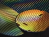
One of the trickiest bits of making semiconductors is photolithography, where light is used to “print” circuits onto silicon wafers. It’s rather like developing a microscopic photograph, except it costs billions and breaks more often.
The process involves spreading a photoresist, a light-sensitive goo, over the wafer. Ultraviolet light then shines through a mask that carries the circuit pattern, and the exposed material is chemically developed so some bits dissolve while others stay put. What remains forms the stencil for the later steps, like etching the metal or silicon layers.
That’s all well and good until the photoresist starts misbehaving. During development, dissolved material sometimes clumps together into microscopic particles that can stick back onto the wafer. At five-nanometre or smaller nodes, even a 30-nanometre blob can ruin a circuit.
it could be this https://www.nature.com/articles/s41467-025-63689-4
My god the headline of the Fudzilla article is misleading.
Yes, they froze the samples of polymer, but the actual change to the technique is to increase the post-emulsion bake!
Much obliged!